
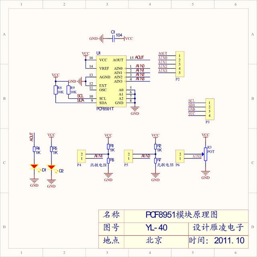
The PCF8591 is a monolithically integrated, and a separate power supply, low-power, 8-bit CMOS data acquisition devices. The PCF8591 has the four analog inputs, one analog output and a serial I2C bus interface.
PCF8591 three address pins A0, A1 and A2 can be used in hardware address programmed 8 PCF8591 device allows access to the same I2C bus, without the need for additional hardware. On the PCF8591 device input and output of the address, control and data signals are transmitted in serial fashion via the two-wire bidirectional I2C bus.
PCF8591 Features
- Single power supply
- PCF8591 operating voltage range of 2.5V-6V
- Via I2C bus serial input / output
- PCF8591 by 3 hardware address pins addressing
- PCF8591 I2C bus speed sampling rate decided
- 4 analog inputs programmable single-ended or differential input
- Automatic incremental channel selection
- PCF8591 analog voltage range from VSS to VDD
- PCF8591 built-in track-and-hold circuit
- 8-bit successive approximation A / D converter
- 1 analog output DAC gain
The easiest way as usual is to purchase a module, I found this interesting one which had integrated devices which can be used to test the analog inputs
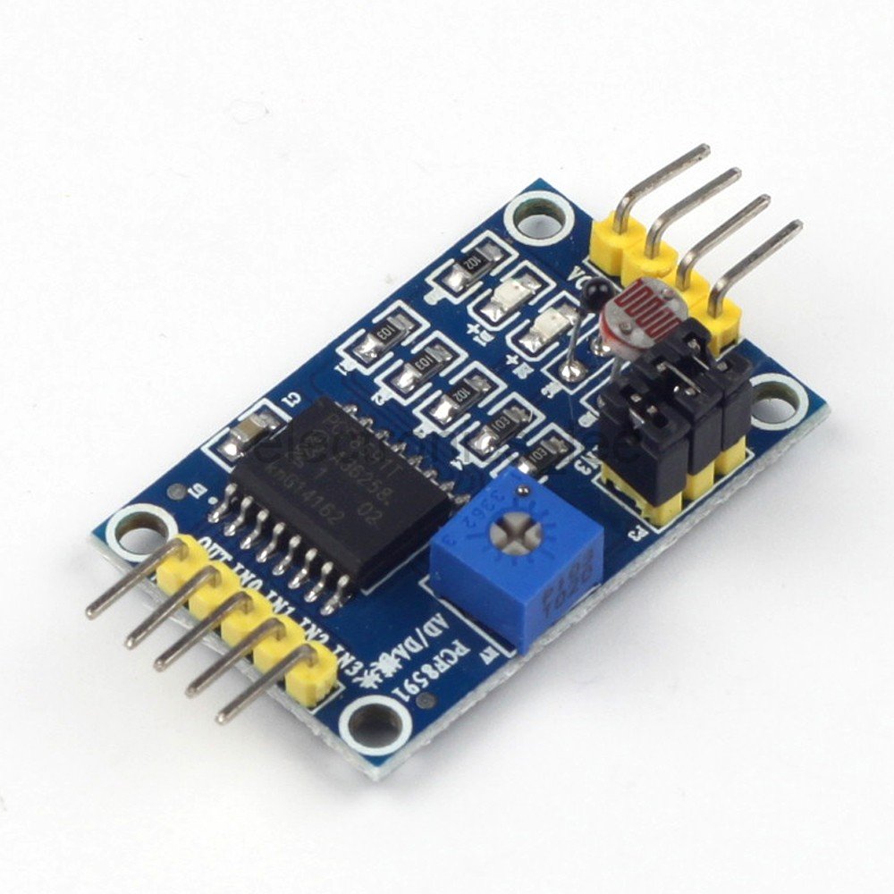
pcf8591 module
Features
- Module supports external voltage input of the 4-way acquisition (voltage input range of 0-5v)
- integrated photoresistor
- integrated thermistor
- integrated potentiometer
- Modules power indicator
- Modules with DA output indicator, when the module DA output interface voltage reaches a certain value, will be lit panel the DA output indicator, the higher the voltage, the more obvious indicator brightness
- Remove shunts to bypass on board integrated devices
The left connector
- AOUT chip DA output interface
- AINO chip analog input interface 0
- AIN1 chip analog input interface 1
- AIN2 chip analog input interface 2
- AIN3 chip analog input interface 3
The right connector
- SCL
- SDA
- GND
- VCC – connected to 3.3v-5v
PCF8591 module functions
| Control | Register | Function | On board Device |
|---|---|---|---|
| 0 | channel 0 | Read ADC 0 | LDR |
| 1 | channel 1 | Read ADC 1 | NTC THERMISTOR |
| 2 | channel 2 | Read ADC 2 | NC |
| 3 | channel 3 | Read ADC 3 | POTENTIOMETER |
| +64 | analog OE | DAC output | O/P LED |
The O/P LED will begin to turn on with the output set to 140 or more with VCC at 3v3.
PCF8591
Parts Required
Here are the parts I used
| Name | Link | |
| ESP32 | 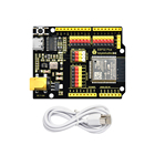 |
|
| PCF8591 | ||
| Connecting cables | 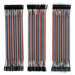 |
Code
#include "Wire.h"
#define PCF8591 (0x90 >> 1)
byte adcvalue0, adcvalue1, adcvalue2, adcvalue3;

void setup()
{
 Wire.begin();
 Serial.begin(9600);
}

void loop()
{
 Wire.beginTransmission(PCF8591);
 Wire.write(0x04);
 Wire.endTransmission();
 Wire.requestFrom(PCF8591, 5);

 adcvalue0=Wire.read();
 adcvalue0=Wire.read();
 adcvalue1=Wire.read();
 adcvalue2=Wire.read();
 adcvalue3=Wire.read();

 Serial.print(adcvalue0);
 Serial.print(" ,");
 Serial.print(adcvalue1);
 Serial.print(" ,");
 Serial.print(adcvalue2);
 Serial.print(" ,");
 Serial.print(adcvalue3);
 Serial.println();

 delay(1000);
}
Output
OPen the serial monitor, adjust the pot, cover the LDR, touch the NTC device and watch the values change
255 ,236 ,255 ,192
255 ,247 ,255 ,180
255 ,238 ,255 ,163
255 ,239 ,255 ,175
255 ,239 ,255 ,222
255 ,240 ,255 ,201
226 ,240 ,255 ,185
131 ,239 ,255 ,188
131 ,239 ,255 ,160
131 ,238 ,255 ,161
131 ,234 ,255 ,158
131 ,238 ,255 ,157
131 ,236 ,255 ,157